I have designed this high voltage, low current power supply for various experiments in systems & synthetic biology. I have cleaned up the design and I am placing the schematic and board layout online below! This circuit outputs up to +1,866VDC at under 1 mA or can be tapped at various points for +622VDC or +933VDC. This is useful for either DIY Biology or institutional research experiments such as:
- capillary electrophoresis
- digital microfluidics using electrowetting-on-dielectric
- possibly electroporation
- various electrokinetic experiments, such as dielectrophoresis
- (other uses?? Let me know)
- and, lastly of course: making huge sparks that go PAHHHHH-POP
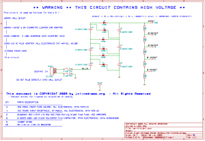
Below is the schematic; read the full post below for the board layout information. Click on the schematic for the full sized version. The schematic operates in stages, so leaving out or bypassing before the 2nd final stage will yield only +933VDC, and leaving out that stage will yield only +622VDC, etc.
The cost of this supply if built using high quality components is under $100. This is a huge contrast to equipment listed in the journal research papers which list scientific supplies costing over $5,000.
For digital microfluidics, the research uses AC or DC. There are some advantages to using AC such as avoiding static charge buildup. However, AC will make droplets oscillate even when stationary.
NOTE: This supply is not suitable for standard agarose gel electrophoresis; the current supplied is not high enough (agarose gel electrophoresis requires >100 mA depending on gel diameter).
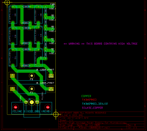
Build this supply at your own risk. The circuit creates high voltages. A screenshot of the board layout is below. Click on the image for a larger version.
To build this board, look at the schematic for the components list. The components are fairly common so can be obtained from different sources. This circuit is the last stage; it connects into a 12V->220VAC auto inverter (the inverter does the big work of creating 220VAC for doubling and tripling).
The design of this circuit is straightforward (following the “Villard cascade voltage multiplier” circuit) and uses the principle of switched capacitors. Each capacitor will only have Vpk voltage across it (the half wave of the AC input) as the diodes are forward biased. When the positive-side diode are reverse-biased when the input AC sine goes negative, the capacitor holds the charge and the opposite leg of the circuit, the negative-side diodes, are forward biased and charge the negative-side capacitors. This creates a doubling after the first stage of 2 x Vpk, and a tripling after the second stage to 3 x Vpk, up to 6 x Vpk in this circuit. Since the capacitors are “small”, the charge capacity and hence the output current is not high. Also, since there are losses in the components, the efficiency will decrease for each stage added, so practically speaking, after a multiplier of 6, a large drop-off is expected — this depends on the components used. The HVOUT voltage potential is measured between the last stage and the AC-VIN ground. Read more about voltage doublers and voltage multipliers at Wikipedia. Larger capacitors will allow for larger current capacity.
The fuses are only for protection during severe component failure, and will not protect the user from getting a significant (and possibly dangerous) zap if the output terminals are touched accidentally. To repeat: Build this supply and use at your own risk.
This circuit is appropriate for systems biology experiments because biology in general does not care about ripple or electrical noise of the output. Scientific supplies are highly regulated and very clean, so the output is very stable. However, it is possible to get away with a simpler, cheaper circuit if ripple doesn’t matter. Many biological operations seem to activate from a wide variety of voltages and charge conditions; usually highly dependent on the particular organism or strain being studied.
Because of the switching action of this circuit, when it’s powered up, it makes a nice BZZZZZZZZZZ sound! This sound is normal.
Make sure to allow this supply to discharge after turning off the power: the capacitors will keep the charge for some time (could be up to 1 minute if no load is connected) and so the supply is still “dangerously live” even after the power has been disconnected. The best method is to disconnect the power and discharge (that means: short through a resistor, for example, 1Meg) the output to ground.
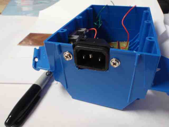
After etching and stuffing the parts, fit the board inside a power box; I picked one up (below is one prototype) from Home Depot and mounted the power recepticle in the side. A power box face plate screws on the front/top. Power connectors (maybe banana plugs – I haven’t populated these yet) will go through the opposite side to be clean, though I’m OK with the wires for now.
The schematic capture and layout was done in KiCAD (open source electronics CAD tool). I made my own footprints for several components, and haven’t figured out how to export these for distribution; eventually I’ll upload them here as a complete package. Leave a comment if you would like the gerber files. The project files below can be used to etch a copper printed circuit board and fill with all the parts. (For newbies to printed circuit boards, search the web for “PCB toner transfer” and “PCB etchant”.)
Project files:
- Schematic in PDF (REVB)
- Board Layout, Copper layer in PDF (REVB)
- Board Layout, Component silkscreen layer in PDF (REVB)
- Board Layout, Component layer in PDF (REVB)
There will be a REVC of this board with improved components in the future (no date set) and at that time I will upload the KiCAD files. In particular the diodes could be upgraded to 1N5062 which has a lower reverse current; and, a front-end transformer could allow output adjustment to create variable DC output.


[…] board (pictured below, using Panasonic PhotoMOS chips), which controls the +930VDC output by the HVPS (posted earlier), and runs over USB using no cost Processing.org software. This is alpha stage testing.. cleaner […]